Low noise Pre-amplifier (Photodiodes)
Page 1 of 1

Low noise Pre-amplifier (Photodiodes)
![]() mdipaolo Mon Mar 09, 2009 1:43 pm
mdipaolo Mon Mar 09, 2009 1:43 pm
I report the outiline of the low noise pre-amplifier that we will use for the photodiodes.
I have studied this circuit with P-Spice.

In the following i report the P-Spice model used in the simulation:
LT1128:
* Copyright ? Linear Technology Corp. 12/21/06. All rights reserved.
* Pinout: IN+ IN- VCC VEE OUT NULL(Pin1) NULL(Pin8)
.SUBCKT LT1128 3 2 7 4 6
IBIASDEF2 0 2 13E-9
IBIASDEF1 0 3 25E-9
RG1 22 0 372400
CG1 22 0 1E-6
GCM2 0 51 50 4 1E-7
RCMRR 51 0 1E3
GPSRR 0 53 7 4 1.78E-8
RPSRR1 53 0 1E3
RVNOI 41 0 1.58E6
DVNF 42 0 DVNOI
IVNF 0 42 1
GG5 0 25 22 0 6.2832
RG5 25 0 0.159155
CG5 25 0 1.5E-6
IDUM1 41 0 0
DVNFX 43 0 DVNOIX
IVNFX 0 43 1
RINX 21 0 0.05675
GG1 0 22 VALUE={9*TANH(V(21))}
MOUT1 77 29 6 6 NOUT
MOUT2 44 29 6 6 POUT
DVL1 23 22 DVLIM
DVL2 23 0 DVLIM
EICM 50 0 VALUE={(V(3)+V(2))/2}
CCMRR 50 52 2.5E-11
RCMRR2 52 51 2k
GIN2 0 21 VALUE={V(101,102)+V(41)+V(42,43)+V(51)+V(53)+1E-5}
GB 0 29 VALUE={3.14*(V(7)+V(4))}
GINOI1 3 0 41 0 1.17E-3
GINOI2 2 0 41 0 1.17E-3
DIN5 2 3 DIN
DIN6 3 2 DIN
GIN1 102 101 3 2 0.035
IIN1 101 4 9E-4
IIN2 102 4 9E-4
RIN1 1 101 3E3
RIN2 8 102 3E3
RIN3 7 1 130
RIN4 7 8 130
GG3 0 27 25 0 0.1
RG3 28 27 10
RG4 0 28 250
LG1 28 0 5E-7
GLIM1 7 77 VALUE={MIN(0.03,(V(7,77)-2))}
GLIM2 44 4 VALUE={MIN(0.03,(V(44,4)-2))}
CIN1 4 3 5E-12
CIN2 2 4 5E-12
GG4 0 29 27 0 6.2832
RG6 29 0 0.159155
CG3 29 0 1.0E-8
ITYP 7 4 5.6E-3
.MODEL NOUT NMOS(KF=0 KP=5 VTO=-1m RD=0)
.MODEL POUT PMOS(KF=0 KP=5 VTO=1m RD=0)
.MODEL DIN D(KF=0 RS=0 IS=1E-16)
.MODEL DVLIM D(BV=18 IS=1E-10 KF=0 RS=0)
.MODEL DVNOIX D(KF=0 RS=0)
.MODEL DVNOI D(RS=0 KF=2E-10)
.ENDS LT1128
IF3602
* ee NJF model
* created using Model Editor release 9.2 on 06/29/08 at 13:27
* The Model Editor is a PSpice product.
.MODEL ee NJF
+ BETA=700E-3
+ LAMBDA=1.0000E-4
+ RD=100
+ RS=100
+ IS=0.5E-9
+ CGD=200.00E-12
+ CGS=100.00E-12
+ KF=1.0000E-18
+ VTO=-3
MoreOVer I report the simulation of the low noise pre-amplifier for the photodiodes.
I think that we can use the circuit in the following condition:
1) G=100 (R24=5 e R2=500 )
2) G=1000 (R24=10 e R2=10k)
In the first and second cases we can choice the better bandwidth:
1)
R1=variable, C1=10n
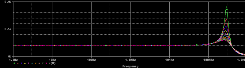
C1=variable, R1=500
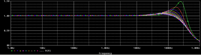
We can use the following values: R1=1k e C1=10n (with G=100)

2)
In the second case, instead, we have: R1=100, C1=1n (with G=1000)
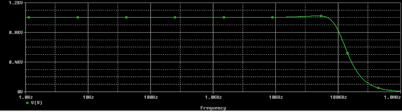
I will try to study the noise of this circuit by mean of SimuLink of MAtLab or also, with but i don't know, P-Spice.
I have studied this circuit with P-Spice.
In the following i report the P-Spice model used in the simulation:
LT1128:
* Copyright ? Linear Technology Corp. 12/21/06. All rights reserved.
* Pinout: IN+ IN- VCC VEE OUT NULL(Pin1) NULL(Pin8)
.SUBCKT LT1128 3 2 7 4 6
IBIASDEF2 0 2 13E-9
IBIASDEF1 0 3 25E-9
RG1 22 0 372400
CG1 22 0 1E-6
GCM2 0 51 50 4 1E-7
RCMRR 51 0 1E3
GPSRR 0 53 7 4 1.78E-8
RPSRR1 53 0 1E3
RVNOI 41 0 1.58E6
DVNF 42 0 DVNOI
IVNF 0 42 1
GG5 0 25 22 0 6.2832
RG5 25 0 0.159155
CG5 25 0 1.5E-6
IDUM1 41 0 0
DVNFX 43 0 DVNOIX
IVNFX 0 43 1
RINX 21 0 0.05675
GG1 0 22 VALUE={9*TANH(V(21))}
MOUT1 77 29 6 6 NOUT
MOUT2 44 29 6 6 POUT
DVL1 23 22 DVLIM
DVL2 23 0 DVLIM
EICM 50 0 VALUE={(V(3)+V(2))/2}
CCMRR 50 52 2.5E-11
RCMRR2 52 51 2k
GIN2 0 21 VALUE={V(101,102)+V(41)+V(42,43)+V(51)+V(53)+1E-5}
GB 0 29 VALUE={3.14*(V(7)+V(4))}
GINOI1 3 0 41 0 1.17E-3
GINOI2 2 0 41 0 1.17E-3
DIN5 2 3 DIN
DIN6 3 2 DIN
GIN1 102 101 3 2 0.035
IIN1 101 4 9E-4
IIN2 102 4 9E-4
RIN1 1 101 3E3
RIN2 8 102 3E3
RIN3 7 1 130
RIN4 7 8 130
GG3 0 27 25 0 0.1
RG3 28 27 10
RG4 0 28 250
LG1 28 0 5E-7
GLIM1 7 77 VALUE={MIN(0.03,(V(7,77)-2))}
GLIM2 44 4 VALUE={MIN(0.03,(V(44,4)-2))}
CIN1 4 3 5E-12
CIN2 2 4 5E-12
GG4 0 29 27 0 6.2832
RG6 29 0 0.159155
CG3 29 0 1.0E-8
ITYP 7 4 5.6E-3
.MODEL NOUT NMOS(KF=0 KP=5 VTO=-1m RD=0)
.MODEL POUT PMOS(KF=0 KP=5 VTO=1m RD=0)
.MODEL DIN D(KF=0 RS=0 IS=1E-16)
.MODEL DVLIM D(BV=18 IS=1E-10 KF=0 RS=0)
.MODEL DVNOIX D(KF=0 RS=0)
.MODEL DVNOI D(RS=0 KF=2E-10)
.ENDS LT1128
IF3602
* ee NJF model
* created using Model Editor release 9.2 on 06/29/08 at 13:27
* The Model Editor is a PSpice product.
.MODEL ee NJF
+ BETA=700E-3
+ LAMBDA=1.0000E-4
+ RD=100
+ RS=100
+ IS=0.5E-9
+ CGD=200.00E-12
+ CGS=100.00E-12
+ KF=1.0000E-18
+ VTO=-3
MoreOVer I report the simulation of the low noise pre-amplifier for the photodiodes.
I think that we can use the circuit in the following condition:
1) G=100 (R24=5 e R2=500 )
2) G=1000 (R24=10 e R2=10k)
In the first and second cases we can choice the better bandwidth:
1)
R1=variable, C1=10n
C1=variable, R1=500
We can use the following values: R1=1k e C1=10n (with G=100)
2)
In the second case, instead, we have: R1=100, C1=1n (with G=1000)
I will try to study the noise of this circuit by mean of SimuLink of MAtLab or also, with but i don't know, P-Spice.
mdipaolo- Posts : 106
Join date : 2008-11-05
» Low Noise Pre-amplifier (Frascati)
» Low Noise Pre-Amplifier
» PDs dark noise and laser noise
» Output Photodiodes
» Closed loop operation
» Low Noise Pre-Amplifier
» PDs dark noise and laser noise
» Output Photodiodes
» Closed loop operation
Page 1 of 1
Permissions in this forum:
You cannot reply to topics in this forum|
|
|